
Due to high-densification, multi-layering, and increase of FPC( Flexible Printed Board), each manufacturing process of the printed circuit board has come to require a high level of measurement management. Furthermore, via infiltration of ISO, traceability-established product guarantees have become necessary, and there is an ever-heightening requirement for reliability in terms of the management of number values. Since Sinto S-Precision developed the printed circuit board-oriented 2-dimentional coordinate measuring machine in 1990, there have been continual contributions towards improvements in the level of printed circuit board measurement management.


-
Creation of a screen mask and film mask which are the original production master of the wiring pattern.


-
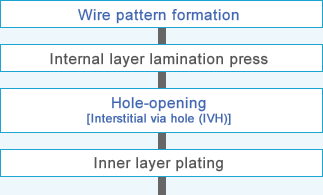
After a pattern is formed on the inner board surface, multiple inner boards are laminated via a press, and for Inner layer connection , interstitial via hole (IVH) process is done, and then plating is done.

-
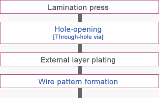
All layers of the board are laminated via a press, and for the purpose of inner layer connection, through-hole via processing is conducted. Afterwards, external plating is conducted, and a wire pattern is formed on the external layer.

-
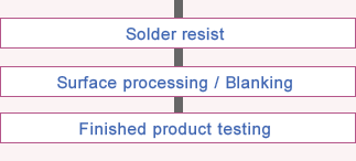
Solder resist is formed upon the board surface, and the surface processing and blanking are conducted, and the printed circuit board is completed. After completion, testing of the finished product is conducted, and then the finished product is shipped out.
*Information here :go to Application for Buildup substrate

Pre- process
- Measurement of artwork process
-
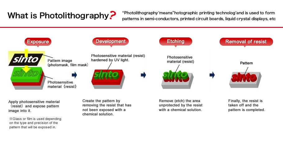
Wiring pattern formation is formed via “photolithography” which involves exposing a pattern through original production master . At this stage, measurement is conducted of the film mask that is primarily used as original production master, and of the screen mask that is created by transcription from the film mask.

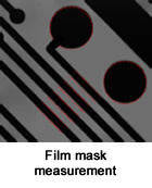
The film mask pattern location, width, interval, diameter and such like are measured. Via the optional software “C-Auto”, creation of a measurement program based upon the CAD data of the pattern’s design data is possible, which improves efficiency. Our company’s equipment can be used for the drawing equipment (plotter) manufacturer’s drawing accuracy evaluation in regard to the drawing of the wiring pattern on the film.
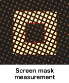
In the screen mask measurement, via image filter functionality and singularity removal functionality, it is possible to conduct accurate measurements that are not influenced by the screen mesh.


Inner ・External layer process
- Measurement of the wiring pattern formation process
-
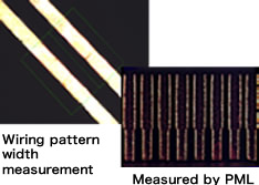
After Copper wiring pattern which formed on the surface of the inner board, the pattern width, interval and location are measured. With the multilayered board, which there are double several pieces internal layer board, every inner layer board are measured.
- Hole-opening process measurement
-
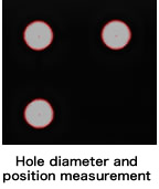
Interstitial via hole (IVH *1 ) processed for inner layer connection and through-hole via processed after lamination of all layer are measured.
- *1 IVH;Interstitial Via Hole
Wiring pattern measurementWidth, interval and position of wiring patterns formed on a board are measured. Because an IC or electronic parts are mounted on the external layer, the position of the surface mount pattern (a pad or land) is also measured.
(Measurement for the position gap of the components mounted by Chip-Mounter is also available.)
Programmable multi-Lighting (PML) is effective to measure top width and the bottom width of the pattern exactly in pattern width measurement.
Hole measurementThe diameter and position of the holes that have been opened primarily via drill processing are measured. With the optional software “C-Auto”, based on drill processing NC data, measurement program authoring can be done, and as such work is made more effective. Additionally, our company’s equipment can also be used for precision evaluation of the drilling machine by machine manufacturers.
Post-process
- Measurement in Solder resist process
-
When printing solder on a pad portion where ICs and electronic components are subject to be equipped later, in order to take care not to solder unnecessary parts, the solder resist layer is coated. At this point, the solder resist position to the pad section is measured.
- Measurement in surface processing and blanking process
-
Via the screen mask or the metal mask, bumps or solder is printed upon the land/pad portion on which electronic components are equipped. At this point, printing-use mask and the printed solder/bump position are measured. Additionally, after the blanking processing (router rocessing), the board’s outline dimensions are measured.
- Measurement in Finished product testing process
-
Finally, as a pre-shipping inspection, measurements are conducted of the designated areas so as to ensure that the product is finished as per the required specifications of drawing.
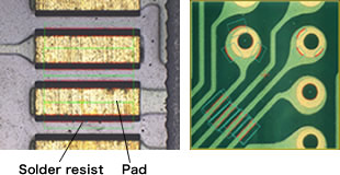
Measurement in Solder resist processSo that malfunctions do not occur when equipping solder-resistant parts to the land/pad section, the solder resist position that is for the land and pad sections is primarily measured. By using the optional color image processing function, the solder resist layer can be confirmed in a clearer image.
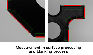
Measurement in surface processing and blanking processAs well as measurement of the dimensions and position of the bumps/soldering printed on the land/pad, by using the optional laser autofocus displacement meter, height can also be measured. In blanking process, various dimension measurements are conducted after groove and V-groove, hole and other processing.
- Measurement in Finished product testing process
At this point, various measurements are conducted, such as external dimension measurement, hole diameter/position, wiring pattern width, and land/pad position.Additionally, with the multipurpose post-processing software “G-Scan2”, it is possible to create an inspection report in any format.
Buildup substrate measurement
A “buildup substrate” which is built via the formation of multiple layers, repeating lamination of each layer to the core board, hole-opening processing, wiring formation, etc. This buildup substrate is more appropriate for high density than multi-layer boards manufactured via conventional processes, and is used for circuit boards that are equipped with LSI, so higher measurement precision is also necessary. Additionally, for connection between the boards, via holes are mainly formed via a laser processor, in which case they are called laser via; the measurement of the laser via is important.
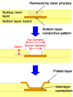
- Laser via measurement
The position/diameter/depth of the laser via that connects directly with the bottommost layer is measured. The depth can be measured via the optional laser autofocus displacement meter, and furthermore it can be conducted until cross-sectional shape confirmation.


