

Used diversely in devices from mobile screens, popularized greatly by the smart phone, to large-size television screens, LCDs have shifted to both high-definition and big-screen specifications. As a result, high accuracy dimension management of LCDs is in demand. SINTO S-PRECISION’s products is used in this manufacturing process in the wide field of LCD measurement. We are especially proud of the top-level track record of the long dimension measurement (total pitch measurement)TFT*1panel and color filter, also corresponding to line width/superposition measurement (CD/Overlay measurement) of LTPS*2 used for high-definition LCDs.
- *1 TFT: Thin Film Transistor
- *2 LTPS: Low Temperature Poly-Silicon


-
The glass substrate (bare glass), which will become the base of the TFT panel and color filter, is created.


-
Stacking several layers of electrodes on the glass substrate, a thin film transistors (TFT) which controls images for each pixel are formed.

-
Red/Green/Blue color is applied to each pixel on the glass substrate.

-
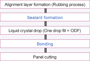
Liquid crystal materials are encased by bonding the TFT panel and color filter together and are then cut to size for the display.

-
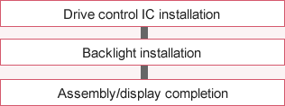
Installation and assembly of surrounding parts is performed to complete the display.
Glass plate process
- Measurement at bare glass manufacturing process
-
At the manufacturing process of bare glass which will be the base for TFT panel and color filter,all types of bare glass dimension measurements are performed.

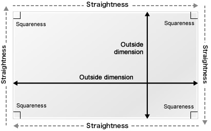
With one piece of equipment, all measurements including the outside dimensions of the bare glass, the squareness of the corners, the straightness of the glass edge and the uniformity of the glass thickness, are possible.


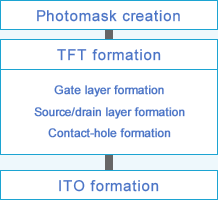
TFT panel process
- Measurement at photomask creation process
-
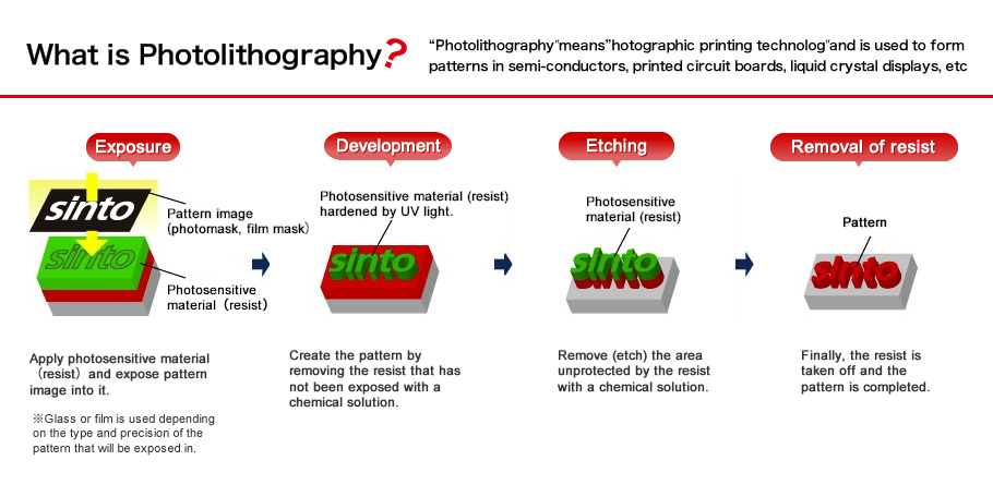
To form the pattern of the TFT and ITO onto the glass substrate, a technology called “photolithography” is used to expose the pattern through glass photographic plate called the photomask. In the process for creating this photomask, the pattern position accuracy (total pitch measurement) and the line width (CD measurement) are measured. For the photomask, which will be the original production master for TFT, a high level of measurement management, higher even that of the TFT panel itself, is demanded.

- Measurement at TFT forming process
-
The TFT, which controls the image of each and every pixel, is formed on the glass substrate.
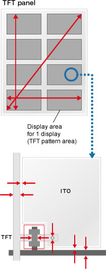
The TFT consists of multiple stacked layers of electrodes. Here, the entire position accuracy of the TFT pattern (total pitch measurement) and of the line width of each electrode, as well as of the superposition accuracy (CD/overlay measurement) are measured. - Measurement at ITO forming process
-
After TFT formation, ITOs (transparent electrodes) are made in each pixel.
Because ITOs must be permeated by backlit light, transparent materials are used. Here, the width of the ITO and the superposition accuracy (CD/overlay measurement) to the TFT are measured.
- Total pitch measurement
The positions of the management marks placed at each display area (TFT pattern area) are measured with high accuracy.The distance between the pattern and position shifting in the pattern (distortion) is confirmed. Because the measurement data is used to correct exposure errors that are fed back to the exposure machine, absolute reliability is demanded of measurement instruments.

- CD/overlay measurement
The TFT is comprised of the gate, source, drain, ITO, etc. CD/overlay measurement is performed for each layer of the TFT and for the contact hole. μ-Master has the software used to accurately detect complex patterns and high-resolution microscopes produced by our company, high-definition LTPS is also measured with absolute accuracy. (SMIC series CD/overlay measurement support specifications are also possible.)

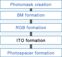
Color filter process
- Measurement of photomask creation process
-
To form the pattern of the BM, RGB and photospacer onto the glass substrate, a technology called “photolithography” is used to expose the pattern through glass photographic plate called the photomask. In the photomask creation process, the position accuracy (total pitch measurement)of the pattern and the pattern line width (CD measurement)is measured. For the photomask, which will be the original production master , a high level of measurement management is demanded.
- Measurement at BM forming process
-
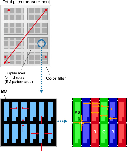
The BM (Black Matrix), which serves as a wall to split the R/G/B colors, is formed into a lattice form on the glass substrate. The BM opening portion is a window through which the light of the backlight passes. The width of the BM and the width of the opening are measured. Also, to ensure that no position shifting occurs when it is bonded with the TFT panel at the cell process, the entire BM pattern is measured (total pitch measurement).
- Measurement at RGB forming process
-
After the BM is formed, pattern formation is repeated three times by photolithography, and RGB color is applied to the BM opening portion. Because backlit light is shone through this RGB, the position shifting in relation to the BM opening portion is measured, so that the RGB color does not mix together.
- Measurement at the photospacer (PS) formation process
-
After formation of the ITO, a protrusion is formed to maintain uniformity of the bonding gap between the TFT panel. Because this protuberance is made with photolithography technology, it is also called a photospacer (PS). The position and width of this PS is measured.
The positions of the management marks placed at each display area (BM pattern area) are measured with high accuracy. The distance between the pattern and position shifting in the pattern (distortion) is confirmed. Because the measurement data is used to correct exposure errors that are fed back to the exposure machine, absolute reliability is demanded of measurement instruments.
BM width, and the opening width are measured together during total pitch measurement. In RGB measurement, by using the color processing function, the RGB width and the shift in relation to the BM can be measured.
Cell process
- Measurement at sealant forming process
-
In order to bond the TFT panel and the color filter, a sealant material is formed by screen printing or application on the portion surrounding the display area. Because liquid crystal material will be put into the inside of the sealant material, uniformity of the sealant material is measured so that it can be sealed completely.
- Measurement at the bonding process
-
After bonding the TFT panel and color filter, a measurement is taken to check whether or not they are misaligned. Since the bonding error fitting marks applied to both panels are measured, this is generally called the fitting measurement.
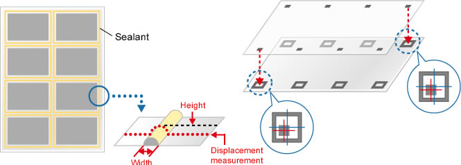
The line width and height of the sealant and the cross-section shape is measured in several places, checking the overall uniformity. The height and cross-section shape is measured by a laser auto focus displacement gauge, produced by company. A 2D or 3D graphic of the cross-section shape can also be displayed. Measurement of screenmask for printing is also supported.
By measuring the position shift of the fitting marks, bonding errors between both the TFT panel and color filter are checked. By measuring in several places, the amount and tendency of shift and rotation is calculated.


