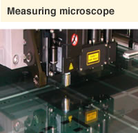
The SMIC-300Ⅲ model converges the essences of the finest 2D plane measuring technologies.
Its credibility in measuring plane coordinates largely exceeds that of traditional non-contact 2D coordinate measuring machines.
Highly-satisfying measurements can be achieved through high-resolution microscopes which enable submicron-level superposition measurement of alignment marks, through technologies in hardware components which constitute SMIC, and through technologies in plane correction.
Recently, SMIC-300Ⅲ has been gaining momentum in MEMS, CMOS sensor and power semiconductor industries .


-
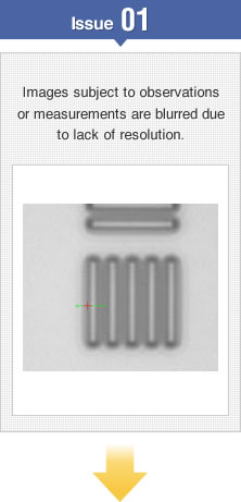
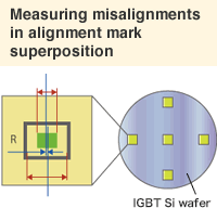
Solved through high resolution microscopes
Using the Company’s optical design technologies, a high-resolution microscope was developed to measure precision of ultrafine patterns.
The microscope captures edge parts of ultrafine patterns (1μm or less) which cannot be captured clearly simply by magnifying. Itcan be used to measure misalignment in superposition of Si wafers or CMOS sensors for IGBT, or dimensions in semiconductor fabrication.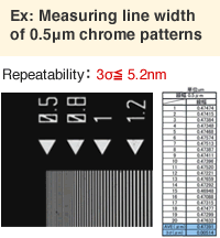

-
Solved through hardware component and plane correction technologies
Granite surface plates & ceramic air sliders constituting SMIC, fiber laser interferometers, and X/Y-axes independent double-column structures driven by linear motors boast long-term stability and enable precise length measurements.
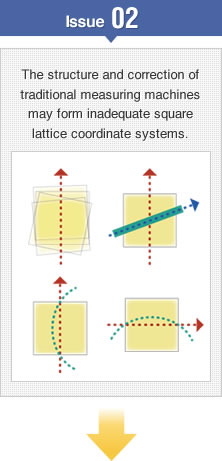
Together with the Company’s correction technology in deploying length corrections from single axes (1D) to surfaces (2D), error causes in length measuring instruments (linear, yawing, straightness, orthogonal) are fully corrected, square lattice coordinates are established, and plane measuring repeatability is ensured.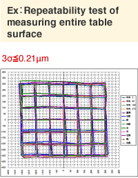

-
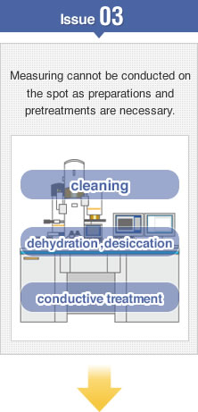
Solved by not requiring pretreatments for vacuum environments or samples
Electron microscopes used for semiconductors must be used in vacuum environments. Since SMIC-300Ⅲ is an optical microscope, it can be used on-the-spot in atmospheric air environments without having to spend time on pretreatments of the objects to be measured. On request, full robotization is also possible.